Become a leader in the IoT community!
Join our community of embedded and IoT practitioners to contribute experience, learn new skills and collaborate with other developers with complementary skillsets.

Join our community of embedded and IoT practitioners to contribute experience, learn new skills and collaborate with other developers with complementary skillsets.


Hey everyone,
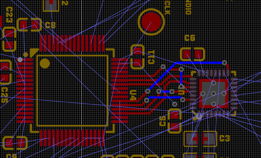
I’m currently working on a PCB design involving the DRV8320 and the STM32G431RBT6TR. As you can see in the attached images, I’m trying to minimize the number of vias between these two components. Ideally, I’d like to have straight traces with minimal or no vias, maintaining the same orientation of the chips.
However, I’m finding it challenging to maintain the necessary functionality, such as BEMF detection with the Virtual Neutral Point and the different comparators for zero-crossing BEMF.
I would greatly appreciate any help or suggestions on how to change the pin assignments while keeping the required functionality intact. Your expertise and advice would be invaluable!
Thank you in advance! @Helper


0Schematic_Done_proto-2024-DRV8320_2024-07-29.pdf
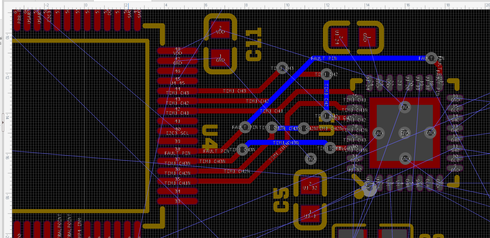
here is how it looks with all the data traces
I would say putting a via in the design isn’t that much of an issue. Vias helps you navigate your route to reach other points.
Yes you’re right but in high power and high speed PCB the vias is a problem because of cross talk and current return
But from what I’ve seen I can reassign the pins
Because the other pins that share the same specification or already used or too far from the driver
@medic4950 I would suggest you consider placing the vias properly to form a pattern, also the size of the vias matters, I see from the picture and schematic that the timer 1 is from pin 34 or so, consider rotating the driver anticlockwise
Thanks for the insights!
hi
sorry for the late reply, I was on holiday.
First, I think the reset pin is missing a pullup resistor.
Before commenting on the vias, I want to know what’s your layer stack up? I think at minimum you should use 4 layers.
You can check out the reference designs by TI, see how they are doing the layout for the DRV chip.
I’d add test points for all signals of interest, especially the gate drive signals.
HI @hemalchevli hanks for the reply and sorry for the delay , So yes it s a 4layer pcb with 2 gnd layer core
the first layer is signal and the fourth one is also a signal
the thickness of the board is 1.6
I have also added some testpoint
but could’t fit them all
here is the design
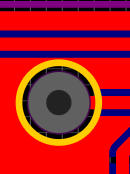
this is a testpoint

in order to find the right size for the vias I’ve used the PCBtoolkit software
here is the view of the software
note that the value that you’re seeing is not the right one
I’m a bit lazy today to re do the manipulation
also I was wondering where should I put the resistor you mentioned
I’ve also reviewed the design recommendations on the TI website for the copper trace sizes and calculated them accordingly.
using the software
I have found out that the signals should be .5mm
Schematic_Done_proto-2024-DRV8320_2024-08-05.pdf
another issue I’m facing Is that I didn’t set up the drc correctly so I have a lot of errors
The pull up resistor on reset, you could place near the pin on IC
Today, I tried to find a way to get straight signals by replacing the pins for Timer 1, but it seems impossible. I confirmed this using STM32 Cube.
since you are using 4 layer with 2 gnd core layers, you can use as many vias as you need
Really!?
yes
nice !
Here is the final version of my board and I don’t think I can optimize it any further.
final-scheme.pdf
DRONE-Nayel.zip
CONTRIBUTE TO THIS THREAD