Become a leader in the IoT community!
Join our community of embedded and IoT practitioners to contribute experience, learn new skills and collaborate with other developers with complementary skillsets.


Join our community of embedded and IoT practitioners to contribute experience, learn new skills and collaborate with other developers with complementary skillsets.


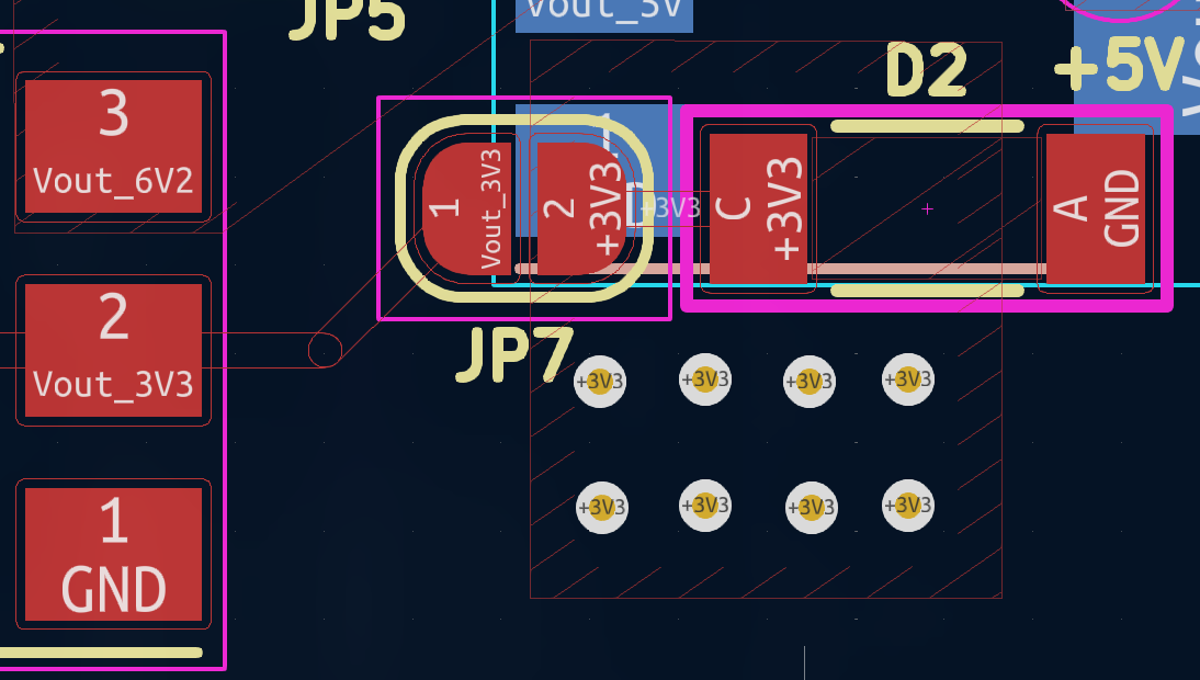
Hey guys! [Please see picture attached ] Request you to comment on my idea of adding vias in my PCB design on the output of the 3v3 linear voltage regulator. Although there is no high current requirement, I still did this just to have a good design. Is this a good rule to follow?


JP7 is a solder bridge to “enable” power to microcontroller
Hello @bruce_wayne5006 there is not need adding vías there, since they are both on the top layer and the connection is straight forward
This is not only for the diode. My question is more about a “good design practise”.
So are you saying this is unnecessary even as a good design practise?
Thanks
It is unnecessary, vias are required to link signals or power from one plane to another. If you are not linking from a plane to another it is not necessary. It is not a good design practice
CONTRIBUTE TO THIS THREAD