Become a leader in the IoT community!
Join our community of embedded and IoT practitioners to contribute experience, learn new skills and collaborate with other developers with complementary skillsets.


Join our community of embedded and IoT practitioners to contribute experience, learn new skills and collaborate with other developers with complementary skillsets.


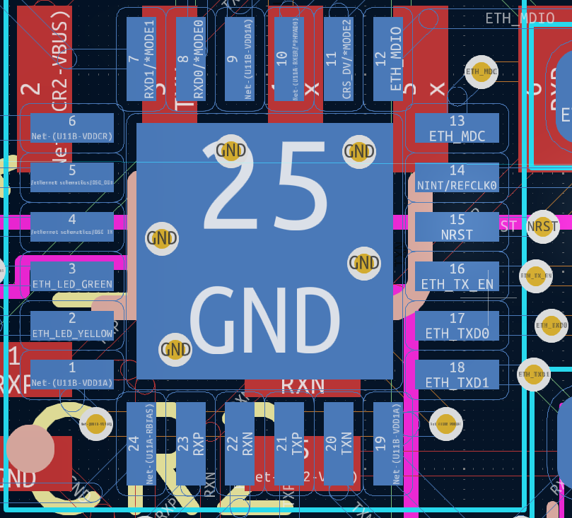
Guys I have a component with QFN package as shown in the picture. Is it okay if I add vias as shown (0.35mm outer, 0.2mm inner) on the ground pad, since I’m not able to route a trace inside? I believe I need to “turn off thermal relief” or something along those lines if I’m doing this. Can someone help me with this please? Thanks in advance @josephogbonna Can you please share your thoughts on this?


It’s fine to do that, you can add more vías to it
Is there any kind of thermal relief settings I need to alter? Normally vias route to the signal from four sides. For the vias placed on the GND pad, do we need to change settings so that it connects to the signal from all sides and not just four?
When you say four sides, you mean the four vías on the ground pad?
Sorry I asked a wrong question without understanding how current passes through the via. I think the entire via’s inner hole circumference will be used to conduct. Conclusion is, I’m slightly worried about any possible issues that might come up if I use via on pads because I read online that we should not do that unless very much required..
It is very much required in your case and very ok to use vias as they connect to the ground directly
CONTRIBUTE TO THIS THREAD