Become a leader in the IoT community!
Join our community of embedded and IoT practitioners to contribute experience, learn new skills and collaborate with other developers with complementary skillsets.

Join our community of embedded and IoT practitioners to contribute experience, learn new skills and collaborate with other developers with complementary skillsets.


Latest step in a MIDI drums project: Displaying MIDI inputs to an Arduino Opta w/ an SSD1306 OLED and my AUX adapter device https://www.tindie.com/products/35482 Wasn’t too hard to get the initial display working, but wow, getting scrolling working like I wanted was a bit of a bear. I used a number of arrays to keep track of each line/value, but had to break up the display and storage into two functions. In fact, I hard-coded the array math into the storeValues function, which most programmers would probably consider pretty poor. Code is on GitHub, FWIW https://github.com/JeremySCook/arduino-experiments/blob/main/MIDI/AutoDrums/OptaAutoDrums.ino


https://www.youtube.com/shorts/tMQWNb_yzHs Project continues to progress. Works well in manual mode as seen here, but I also have an automatic mode that goes through a drum pattern.
What got me stuck (and it still is not perfect, as it’s using a blocking/delay() function in auto mode) is that if the solenoid isn’t triggered for long enough it won’t fully extend all of the time.
I bumped it up to 50 milliseconds per a previous project, and also added a 2200uF capacitor between the + and – supply and now it seems to work well.
So I guess the lesson is that solenoids aren’t instantaneous… As obvious as that might be now, ha.
OTOH, it’s hard to argue with getting something to work, so I’d call it passing if not an A+. Ha!
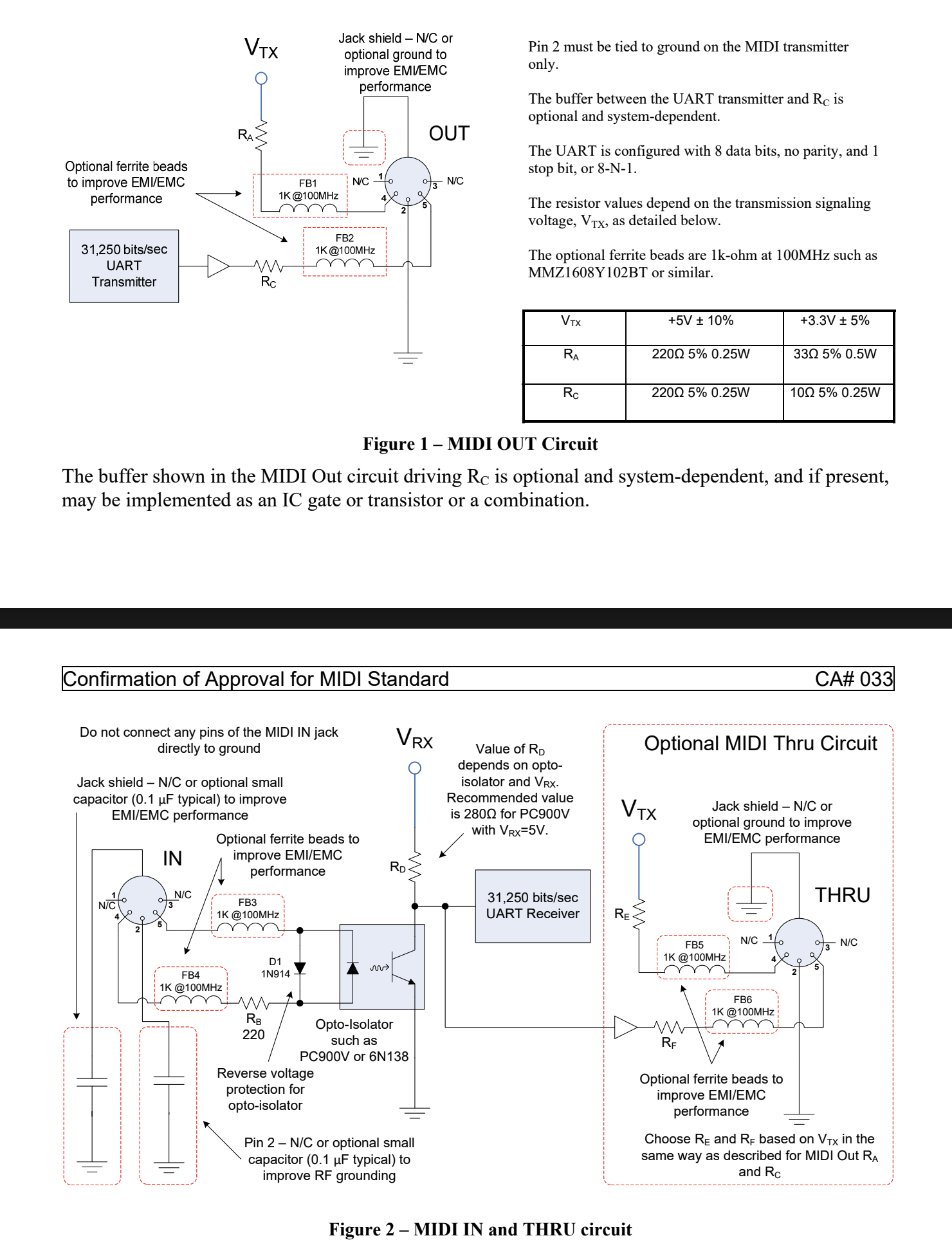
Considering doing a MIDI pass-thru device based on this spec: https://midi.org/5-pin-din-electrical-specs. Interestingly, the thru circuit shows a buffer, which is optional on the MIDI output spec, but not explicitly stated as optional there. Think leaving it out is OK? Guessing so, but not sure what the letter and/or intent of the “law” is here.
The overall device, as I envision it, would pass MIDI signals though, but read them as well and display on a little OLED screen for diagnostics etc. I’d probably use an ATtiny85… So if it needs a buffer, coudl an ATtiny85 act as one? Seems like it could. Interested in people’s thoughts.

The MIDI spec in the diagram you’re referencing shows a buffer in the “Thru” circuit as a non-optional element, unlike the output circuit where it’s marked optional. However, you can likely leave it out, as many MIDI circuits function without explicit buffers if signal degradation isn’t an issue.
An ATtiny85 can act as a buffer depending on how it’s configured. It has enough GPIO pins to handle basic MIDI input and output, and if you’re adding an OLED display, you can manage the signal processing and pass-thru functionality with some clever coding.
In short: skipping the buffer should be fine for most setups, but if you notice signal issues, consider adding it later. The ATtiny85 could act as a buffer with the right setup.
Interesting, yes, I suppose having the buffer would be the spec. Assuming that was the intention, I wonder if it has to do with MIDI being designed to really isolate things well. I guess if it is a product I’m going to sell, which it might be, I’m a little leery of calling it “MIDI” if I don’t match the spec perfectly… though it might not matter.
As far as configuring it as a buffer, it that a matter of programming it to do so, e.g. – this input = this output, or is there some other low-level way to take care of this? Given 2 pins for I2C, 2 pins for MIDI in/out, and maybe a status LED that’s pretty tight IO-wise. As it always is with an ’85, which is sometimes what makes it fun-ha.
Considering diving into the world of 4-layer boards for this MIDI processing/pass-through application, meaning that any signals that I pass will transmit at 31,250 baud. I don’t think the board will be that difficult to design circuitry-wise, but what is the prevailing idea for how to stack the layers in such a board?
Thinking maybe GND, Signals, GND, Power would provide the best noise immunity and make it really easy to access the power that I need. OTOH, having multiple GND planes might also mean GND loops from what I understand… though my *understanding* of said loops is rather vague. Guess I’d need to pass some vias though the GND sandwitch.
Anyway, open to ideas/standard practice here.
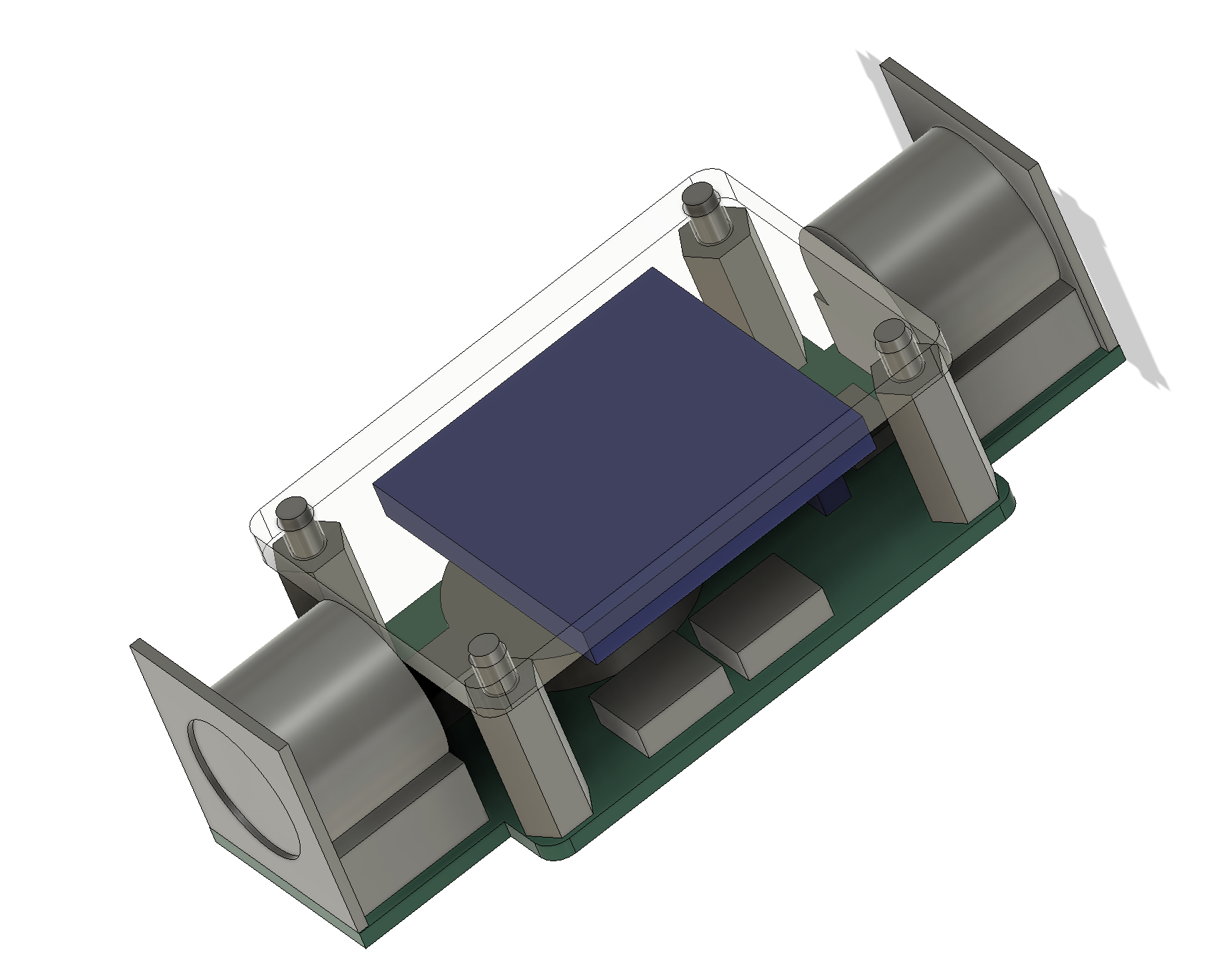
My preliminary CAD model w/ MIDI in and MIDI out

How about using signal ground ground signal. This provide more noise immunity. You can always route the power rails. But if you have multiple power rails then I suggest you use a power plan for that
The most common stack up for 4 layers is
Signal
GND
Power
Signal
But I don’t t use it becauseI prefer not to change the reference layer when switching signals from top to bottom.
I prefer to use this
Signal
GND
GND+Power
Signal
In the above stack up, make sure the signal and power traces don’t cross, there must always be GND plane below the signal trace.
Thanks for the input. What do you mean by reference layer? Do you mean the face that you’ve got signal right below power on the most common layout?
The way you have it seems to make sense – do you also fill the empty areas in the signal layers with GND or do you leave that blank?
Part of me thinks putting GND on both outside layers would be nice for RF concerns, but I imagine there are some real problems with that. I suppose to physically connect to your components you’d need vias each and every time.
Yes, that’s right reference plane is the plane right below the trace.
Yes, I do fill in the empty areas on top and bottom with ground, bonus point if you also add stitching vias connecting GND on all 4 layers, minimizing the GND loops.
CONTRIBUTE TO THIS THREAD