Become a leader in the IoT community!
Join our community of embedded and IoT practitioners to contribute experience, learn new skills and collaborate with other developers with complementary skillsets.


Join our community of embedded and IoT practitioners to contribute experience, learn new skills and collaborate with other developers with complementary skillsets.


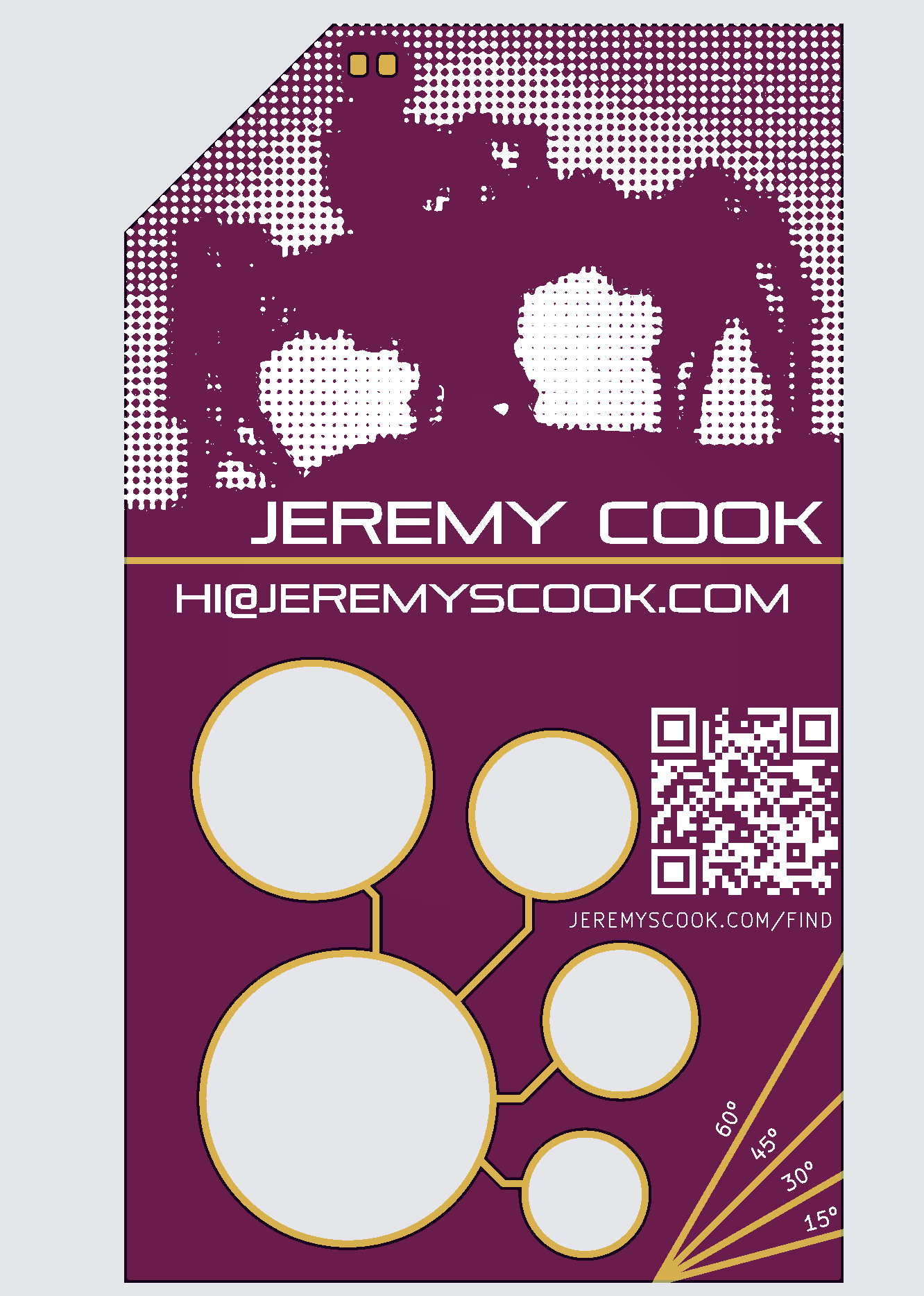
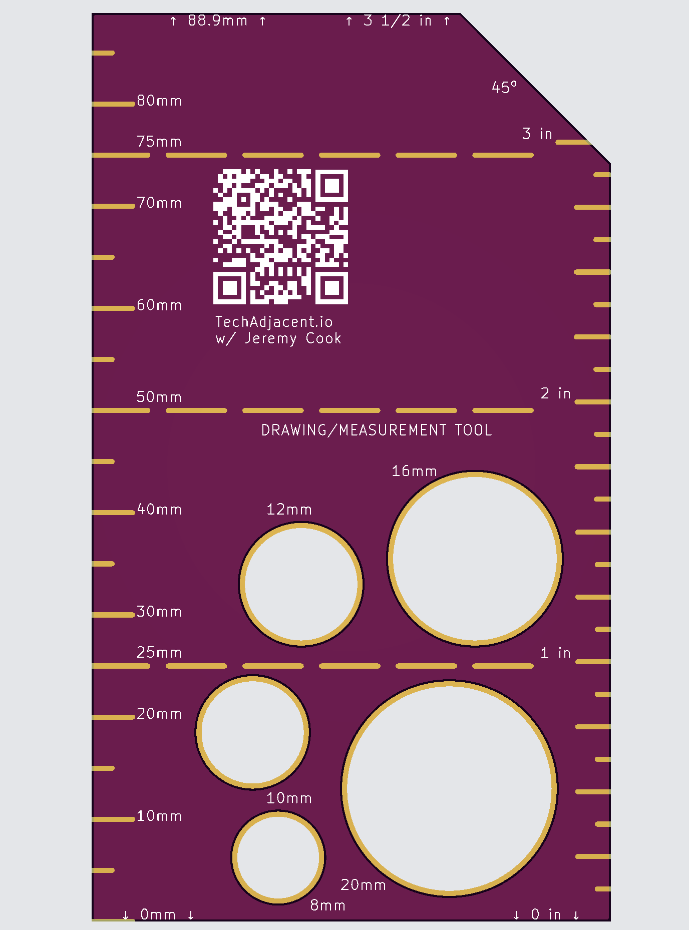
My PCB business card/measurement tool continues to evolve. Added angular markers on the top surface, and reduced the copper to edge clearance (Board Setup > Design Rules in KiCad) to .2mm so that the inch/mm marks on the back (no solder mask) would be closer to the edge.
Made a few other little changes too, but the big one is that I am going to order it in purple and ENIG via JLCPCB. Also planning to do matte black/ENIG later with PCBWay and eventually compare things on https://www.techadjacent.io/ – Haven’t ordered yet, so LMK if you have any suggestions!


CONTRIBUTE TO THIS THREAD